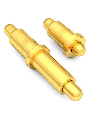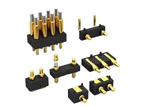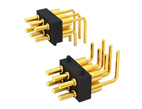


A reliable pogo pin connection starts with coordinated electrical, mechanical and PCB design. Engineers must define the current, signal type, working stroke and alignment tolerance before finalizing pad dimensions or pin spacing. Correct land patterns, controlled compression and an appropriate mounting method help prevent unstable contact, solder cracking, excessive wear and assembly failures.
Start With the Electrical and Mechanical Design Requirements
Before drawing the footprint, determine what the connection must carry and how it will move. A PCB pogo pin used for low-current testing has different requirements from one that transfers charging current or operates through thousands of compression cycles.
The initial specification should include:
Electrical load: voltage, continuous current, peak current and signal type
Contact resistance: acceptable initial resistance and resistance after cycling
Mechanical life: expected number of compression cycles
Working height: distance between the PCB and mating surface during operation
Spring force: force per pin and total force across the connector
Environment: operating temperature, vibration, humidity, dust and corrosion exposure
Assembly process: reflow soldering, wave soldering or manual soldering
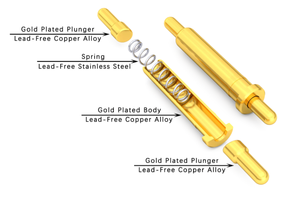
The connector arrangement also depends on the direction of contact. Standard pins usually connect a PCB to a flat contact pad, while double sided pogo pins can create spring-loaded contact at both ends in board-to-board, modular or replaceable assemblies.
Define these requirements before selecting a part number. Changing the pin diameter, travel or mounting type after the PCB layout is complete can require a new footprint, housing and tolerance analysis.
PCB Pad Layout, Pitch and Keep-Out Area
The PCB land pattern should follow the dimensional drawing and recommended footprint for the selected part. Do not design a generic pad and assume that it will fit every pogo pin with a similar barrel diameter.
For an SMD design, the pad must provide enough area for a stable solder joint without creating excessive solder movement during reflow. The layout should account for the pin terminal size, solder fillet, solder mask opening and placement tolerance. Excessive solder paste can allow the pin to tilt or float, while insufficient paste may create a weak joint.
For through-hole designs, confirm:
Finished hole diameter and pin-tail tolerance
Annular ring dimensions
PCB thickness and hole plating
Required solder fill
Clearance around nearby traces and components
Pitch is the center-to-center distance between adjacent contacts. It must provide space for the pin body, housing walls, assembly tolerance and electrical clearance. High-current contacts may also need wider copper traces and more spacing for heat dissipation. For signal contacts, routing rules may need to consider crosstalk, ground placement and impedance requirements.
A keep-out area should be reserved around the contact array for the connector housing, pin movement, solder inspection and assembly tools. Components should not interfere with the mating device or prevent access for rework. Mechanical drawings should show both the uncompressed and working positions of the connector.
Working Stroke, Compression and Alignment Tolerance
A pogo pin normally has a free height, maximum travel and recommended working stroke. These values are not interchangeable. The pin should operate within the supplier’s recommended compression range rather than being designed to reach full travel during normal use.
Too little compression can produce insufficient contact force, unstable resistance or intermittent signals. Too much compression can overstress the spring, accelerate plating wear, damage the mating pad or transfer excessive force to the solder joint and PCB.
The required compression should be checked using a tolerance stack that includes:
PCB thickness and flatness
Pin height tolerance
Housing and mounting tolerance
Mating-pad position
Enclosure deformation
Assembly gap variation
The worst-case minimum compression must still establish reliable contact, while the worst-case maximum must remain below the permitted travel.
Alignment is equally important. Pogo pins are intended primarily for axial movement. Side loading can cause the plunger to bind, scratch the mating surface or wear unevenly. Lead-in features, guide holes, locating posts or a floating housing can help align the two assemblies before the pins are compressed.
SMD, DIP and Through-Hole Mounting Methods Compared
The mounting method should match the available PCB space, production process and mechanical loading. For automated assembly, RTENCH’s pogo pins smd range provides surface-mount options that can be integrated into an SMT production line. Their footprints and reflow conditions still need to be verified for the selected model.
| Mounting Method | Main Advantages | Primary Design Concerns |
| SMD | Compact layout and automated placement | Pad size, paste volume, coplanarity and side-load resistance |
| DIP | Good PCB retention and straightforward positioning | Hole tolerance, solder fill and space on both PCB sides |
| Other through-hole terminals | Strong mechanical support for repeated operation | Board thickness, annular ring and soldering process |
In pogo pin catalogues, DIP normally refers to a type of through-hole terminal, while THT is the broader assembly category. The exact tail structure should therefore be confirmed from the product drawing rather than from the mounting label alone.
Additional mechanical support may be necessary when the connector experiences repeated impacts or lateral force. A plastic housing, locating feature or mounting bracket can absorb stress that would otherwise reach the solder joint. More detailed pogo pin mounting instructions should be reviewed before establishing the assembly process.
Common PCB Design and Soldering Failures
Many connection failures result from interaction between the footprint, mechanical assembly and soldering process rather than from the pogo pin alone.
| Failure | Likely Cause | Recommended Correction |
| Pin tilts after reflow | Uneven paste, oversized pad or poor placement support | Optimize the footprint, stencil opening and placement process |
| Intermittent connection | Insufficient compression, contamination or misalignment | Review the tolerance stack and mating interface |
| Solder joint cracks | Side loading or repeated mechanical stress | Add housing support and improve alignment |
| Excessive temperature rise | High resistance, narrow traces or insufficient copper area | Measure resistance and improve current routing |
| Uneven pin heights | PCB warpage, placement variation or floating during reflow | Improve coplanarity control and assembly fixturing |
The reflow profile must remain within the component’s temperature limits. For through-hole parts, verify soldering temperature, exposure time and hole fill. Flux residue or contamination around the plunger should be avoided because it can interfere with spring movement and increase contact resistance.
Before mass production, inspect solder joints and measure contact resistance across the complete assembly. Functional testing should reproduce the intended compression, current and mating cycles. Thermal testing is especially important for charging and power-transfer applications.
FAQs About Pogo Pins in PCB Design
How large should a PCB pad for a pogo pin be?
Use the recommended footprint for the exact model. The correct size depends on the terminal dimensions, mounting method, solder fillet, stencil design and placement tolerance. A generic pad size is not suitable for every pin.
How is the correct pogo pin pitch determined?
Pitch must accommodate the pin diameter, housing structure, assembly tolerance and electrical-clearance requirements. Current level, heat dissipation and signal integrity may require more spacing than the minimum mechanical pitch.
How much should a pogo pin be compressed?
Design around the supplier’s recommended working stroke. Check both minimum and maximum compression through a complete tolerance-stack calculation, and avoid using full travel as the normal working position.
Are SMD pogo pins suitable for repeated mating?
They can support repeated mating when correctly selected and mechanically supported. Alignment features should prevent side loading from being transferred directly to the surface-mount solder joints.
What information should be provided for a custom PCB pogo pin connector?
Provide the pin count, pitch, current, signal type, working height, stroke, spring force, mounting method, mating-cycle target, PCB layout restrictions and environmental requirements. PCB and enclosure drawings help the supplier evaluate the complete interface.